Quick Facts
Biography
Donald Lee Klein (born December 19, 1930) is an American inventor and chemist, most known for inventing the process to fabricate the self-aligned gate MOSFET transistor along with Robert E. Kerwin and John C. Sarace in 1967 at Bell Labs.
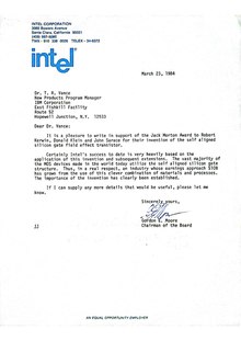
In 1994, together with Kerwin and Sarace, Klein received the IEEE Jack A. Morton award (renamed in 2000 to the IEEE Andrew S. Grove Award) "For pioneering work and the basic patent on the self-aligned silicon-gate process, a key element in fabrication of very large scale integrated circuits."
That same year, Klein, Kerwin and Sarace were declared "Inventors of the Year" by the New Jersey Inventors Hall of Fame.
Early life
Klein was born in Brooklyn, New York to Kalman Klein, a Hungarian Jew who immigrated to the United States at age 16, and Emily Vogel, an American born Austro-Hungarian Jew.
Donald's brother Herbert, who was 7 years older, was a radio amateur from a young age. He served in WWII as a radio operator on a ship for the Navy.
For Donald's 13th birthday, Herbert gave him his first chemistry set (which he obtained through his Electrical Engineering studies).
Klein began experimenting with the chemicals, while collecting more from family members and buying his own. Eventually he had built his own laboratory in his parents' basement.
After high school, Donald followed in his brother's footsteps, becoming a licensed radio amateur.
Education
In 1945, Klein attended Brooklyn Technical High School where he took many chemistry courses including inorganic, qualitative and quantitative analysis, organic chemistry, physical chemistry and chemical engineering.
After high school, Klein attended Polytechnic Institute of Brooklyn (now New York University Tandon School of Engineering). After briefly debating between Metallurgy and inorganic chemistry, Klein decided to major in inorganic chemistry. Eager to combine his passions of chemistry and electronics, Klein decided to research radio frequency titrimetry for his undergraduate thesis, a new field at the time.
Upon graduation, Klein began working at Sylvania Electric Products Inc. in Boston, Massachusetts to support his new family (he got married one week after graduating). Klein enjoyed his time at Sylvania where he was able to combine his passions for electronics and chemistry, working on solid-state electronics. During his time at Sylvania, Klein wrote numerous articles for QST about semiconductor device applications.
After 2 years at Sylvania (which Klein refers to as his "post-graduate education"), Klein decided to pursue a graduate degree at the University of Connecticut working with Dr. Roland Ward who he'd met during his undergraduate studies. Ward, often considered the father of solid-state chemistry, had moved from the Polytechnic Institute of Brooklyn to the University of Connecticut. Klein's research with Ward, which focused on photochemistry was published in the Journal of the American Chemical Society.
In 1958, Klein graduated from the University of Connecticut with a PhD in inorganic chemistry.
Career

"A $30 billion+ industry with this today!"- Moore
"This is the invention which made VLSI a practical reality!"- Noyce

In 1958, Dr. Ward introduced Klein to a headhunter from Bell Labs who was eager to recruit Klein. Klein Joined Bell Labs in November, 1958. Although he was originally recruited to join the chemistry research department, Klein began working in the chemistry development department where he worked on the development of semiconductors.
Klein was thrilled to be working along some of the brightest chemists in the world. As Klein said during an interview with the Chemical Heritage Foundation, "There were more experts under that one roof at Murray Hill, than at any university that I had ever been to, or have been in since. You could always find an expert in every single field you could think of." Klein referred to his time at Bell Labs as "the greatest post graduate education I ever had."
Along with his colleagues, Klein worked to develop etching techniques and ways to prevent contamination in the process of semiconductor production.
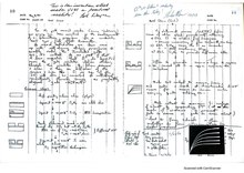
In February 1966, Willard Boyle, a high level manager at Bell Labs, posed a problem to Klein. At the time, the production process of integrated circuits required 6 or 7 steps, each with a yield rate of below 90%, resulting in unacceptably low yield rates. What was desired was a process that would be go/no-go, meaning a process in which an entire batch of wafers can be eliminated early on in the production process. Following his discussion with Dr. Boyle, Klein led a brainstorming session with several other Bell scientists to design a better process for building FET devices. Out of that meeting came the idea of using a heavily doped polycrystalline silicon layer as the gate of an FET. The gate was to be supported on dual layers of a silicon nitride and silicon dioxide serving as the gate insulator. Using the FET as a model for integrated circuits, they fabricated and characterized hundreds of FET devices at high yield that exhibited close electrical tolerances.
Klein and his group published numerous papers on this new technology and also patented the process.
Klein remained at Bell Labs until 1967, when he joined IBM. Before joining IBM, an agreement was made between Bell Labs and IBM that Klein would not be allowed to work intimately on the problems that he had been working on at Bell Labs, for at least a period of time.
Unable to work directly on MOSFET technology, Klein was asked to set up a group to advance the technology of lithography. More specifically, Klein's group worked on developing new photoresist technologies.
While at IBM, Klein worked as a senior engineer, manager, and technical staff consultant.
In 1987, Klein retired from IBM and began teaching chemistry at the department of physical sciences at Dutchess Community College in his hometown Poughkeepsie, New York.
Patents
- Method of fabricating semiconductor contacts, (1965).
- Semiconductor surface cleaning, (1965).
- Method for the preparation of atomically clean silicon, (1969).
- Silicon oxide tunnel diode structure and method of making same, (1969).
- Method for making MIS structures, (1969).
- Cyclic polyisoprene photoresist compositions, (1972).
- Device for removing low level contaminants from a liquid, (1977).
Personal life
In 1952, Klein married Ruth Kintzburger (also a chemist and radio amateur), a childhood friend from Brooklyn. Together they had 6 children and 21 grandchildren.

 Sagittarius